Technology
Lumics develops, manufactures, and markets semiconductor laser diodes, laser modules and diode laser systems for medical & life science, industrial, analytical & sensing, and pumping & seeding applications. The company has invented, patented and utilizes a novel manufacturing process for laser diodes which provides highest power density and reliability for high power laser diodes over a wide range of wavelengths from 750nm to 2000nm.
Lumics’ technology is particularly suited for high-power laser diodes. Consequently, it has experienced particular strong reception of its laser modules in the growing market for high-power medical and industrial diode lasers.
Lumics chip technology
The Lumics patented chip technology includes a proprietary laser diode facet passivation procedure. The chip design and the manufacturing process have been highly optimized over the last 20 years. The key features of the Lumics chip are summarized as follows:
- The Lumics laser diodes are edge emitting ridge waveguide lasers, which is the proven and accepted concept of choice for very high power single mode and broad area applications.
- In order to ensure long life-time of the GaAs/AlGaAs based laser diodes the front and rear chip facet must be passivated to avoid degradation and catastrophic optical mirrow damage (COMD). Lumics has developed a process which allows to form a perfectly crystalline and virtually defect free passivation layer on the chip facet. This is the best in-class mirror protection. Its main purpose is to avoid light absorption, which would result in facet heating and oxidation of the Al-containing laser material.
- The perfect crystalline passivation layer is non-absorbing down to very short wavelength of less than 750nm. Therefore, the Lumics chip technology offers high flexibility in wavelength.
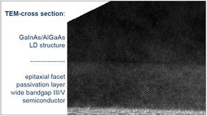 Figure 1: Cross sectional transmission electron microscopic image of the crystaline facet passivation layer on the surface of the laser diode chip facet.
 - The Lumics laser diodes are based on the GaAs/AlGaAs heterostructure with InGaAs or GaInAsP active quantum well layers depending on wavelength. The GaAs/AlGaAs compound semiconductor is the preferred material combination for highest power applications compared to Al-free materials, because of its superior intrinsic physical properties such as carrier confinement, thermal and electrical conductivity, and the possibility to allow more flexible refractive index variation in the waveguide design.
The main problem of AlGaAs is oxidation and defect generation on the chip facets after exposure to air. However, Lumics can take full advantage of the GaAs/AlGaAs material due to its unique facet passivation technique.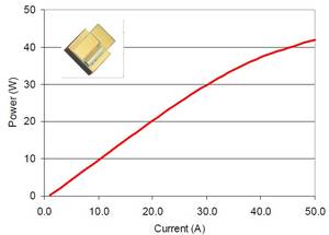
Figure 2: Optical output power vs. current in pulsed operation (13 µsec pulse 6.6 KHz) for a 94µm emitter with 915nm wavelength on Flat_mount (see insert).
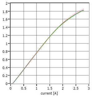
Figure 3: Optical output power vs. current, c.w. operation of 980nm single mode laser diodes. The graph shows a batch of 16 laser diodes.
In summary, the Lumics technology with its facet passivation potentially allows highest power density with more flexibility in wavelength. Figure 2 shows the power vs. current characteristic for a 94µm wide broad area emitter on submount with 4.4mm chip length. The laser diode on submount is shown in the insert. The device is operated in pulsed mode with 13µsec pulse and 6.6kHz. The maximum peak power exceeds 40W at 25°C base temperature. This is to our knowledge the highest peak power currently reported for a 100µm single emitter. Figure 3 shows the optical output power vs. current in c.w. operation for 16 pcs of 980nm single mode laser diodes. More than 1.8W are reproduceably achieved with very high lifetime.
Both the broad area and the single mode data shown in Figure 2 and 3 clearly indicate the extremely high COMD level of the Lumics laser diodes.


